Introduction:
The global Probe Card Market is projected to reach over USD 4.8 billion by 2030, growing at a CAGR of 6.9% from 2024. Probe cards are essential components in semiconductor wafer testing, directly impacting device performance, yield, and cost. The growing complexity of integrated circuits (ICs), increasing demand for consumer electronics, and the evolution of advanced packaging technologies are fueling market expansion. Rising production of memory chips, microprocessors, and 5G components has heightened the need for accurate and efficient wafer testing, positioning probe cards as critical tools in ensuring chip functionality and quality in high-volume manufacturing environments.
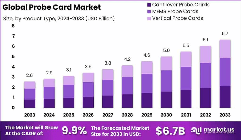
Key Takeaways:
- Market to reach USD 4.8 billion by 2030
- CAGR of 6.9% driven by semiconductor complexity and demand
- Critical role in wafer-level testing of ICs
- Increasing use in memory, logic, and RF chips
- High demand from consumer electronics and 5G deployment
- Advanced probe card types like vertical and MEMS are gaining traction
- Asia-Pacific remains the manufacturing hub and leading adopter
- Higher pin count and fine-pitch technologies are rising
- Automotive and AI chips create new testing demands
- R&D investments boosting multi-die and stacked chip testing
Emerging Trends:
MEMS-based probe cards are emerging as a key technology for high-density and high-frequency testing. Adoption of vertical probe cards is increasing to accommodate complex 3D IC architectures. Probe cards with active thermal control and self-diagnosis features are becoming prevalent. AI-driven wafer inspection is enhancing test automation. Fine-pitch and ultra-fine pitch probe cards are in high demand to match next-gen node advancements. Use of laser technology and photonics in probe designs is growing. Custom probe cards are being developed for advanced logic and mixed-signal applications. Increasing focus on sustainable, longer-life probe card materials is underway. Chiplet and heterogeneous integration are reshaping design needs.
Use Cases:
- Testing of memory ICs, including DRAM and NAND flash
- Quality assurance in CPU and GPU wafer production
- RF device testing for mobile and wireless communication
- Wafer-level testing in automotive-grade semiconductors
- Testing of advanced packaging like 2.5D and 3D ICs
- Quality control for AI, ML, and data center processors
- Final wafer inspection before die singulation
- Rapid testing of chips for smartphones, tablets, and laptops
- Wafer acceptance testing in outsourced semiconductor assembly and test (OSAT)
- Development and characterization testing in R&D labs
Major Challenges:
Maintaining precision at micro and nano levels as IC geometries shrink is increasingly difficult. Higher pin count and tighter pitch increase probe complexity and potential for yield loss. Rising test costs impact profitability for semiconductor manufacturers. Material fatigue and probe tip wear affect test accuracy and life span. Integration with high-speed ATE systems requires robust compatibility. Rapid technology evolution demands continuous probe card design adaptation. Lack of standardization across chipmakers complicates customization. Delicate wafers can be damaged during probing, leading to lower yields. Testing stacked or chiplet-based architectures adds structural complexity. Global supply chain disruptions can affect timely probe card delivery.
Opportunities:
Growing demand for 5G, AI, and IoT semiconductors creates opportunities in high-frequency, high-density probing. Expansion of automotive electronics and autonomous systems increases the need for ultra-reliable testing. Heterogeneous integration and chiplets offer new design and test challenges. Advanced packaging techniques like fan-out and 3D stacking boost demand for innovative probe cards. Emerging applications in biomedical and industrial IoT create niche markets. Digital transformation in testing facilities drives interest in smart and predictive probe card technologies. Increasing semiconductor fabs in Asia and the U.S. boost regional market growth. Customization and probe-as-a-service models create monetization paths. Collaborations with ATE vendors improve system-level optimization.
Key Players Analysis:
The probe card market is shaped by a mix of large semiconductor test solution providers and niche probe card manufacturers. These players focus on innovation in MEMS technology, fine-pitch capability, and high-speed probing. Strategic alliances with foundries, fabless companies, and OSATs enable deeper integration into production workflows. Competitive differentiation is based on probe accuracy, durability, thermal control features, and compatibility with advanced nodes. R&D efforts emphasize multi-die, 3D ICs, and wafer-level chip scale packaging. Players increasingly offer co-engineered solutions with ATE systems. Custom design services and quick-turn manufacturing are key advantages. Focus areas include RF, automotive-grade, and AI chip testing applications.
Conclusion:
The probe card market is a vital enabler of the semiconductor industry’s relentless innovation, ensuring accuracy and quality in ever-smaller and more complex devices. With demand rising across 5G, AI, automotive, and advanced computing sectors, probe card technologies must evolve rapidly. Despite challenges like increasing complexity and cost, the market is buoyed by advancements in MEMS, fine-pitch design, and adaptive testing solutions. As chip architectures diversify and packaging evolves, the role of precision testing becomes even more critical. The probe card market is well-positioned for sustained growth, driven by its indispensable function in semiconductor manufacturing’s future landscape.
The macro analyst desk brings highly sought after financial news based on market analysis, insider news and company filings.