Global Semiconductor EUV Photomask Inspection Equipment Market Outlook 2025: Key Trends, Growth Opportunities, and Strategic Forecast
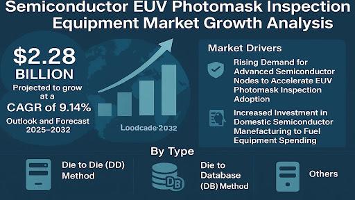
Global Semiconductor EUV Photomask Inspection Equipment Market size was valued at US$ 1.15 billion in 2024 and is projected to reach US$ 2.28 billion by 2032, at a CAGR of 9.14% during the forecast period 2025-2032.
Semiconductor EUV photomask inspection equipment plays a critical role in semiconductor manufacturing by detecting defects in extreme ultraviolet (EUV) lithography masks. These high-precision systems utilize advanced imaging technologies such as electron beam inspection and actinic inspection to identify pattern errors, particles, and other imperfections that could affect chip performance. The equipment is essential for maintaining yield rates in advanced node semiconductor production.
The market growth is driven by increasing adoption of EUV lithography for sub-7nm chip manufacturing and rising demand for high-performance computing devices. While the COVID-19 pandemic caused temporary supply chain disruptions, the market has rebounded strongly due to accelerated digital transformation across industries. Key players like KLA Corporation and Applied Materials continue to innovate, with recent product launches featuring improved throughput and sensitivity for 3nm and below process nodes. Asia-Pacific dominates the market, accounting for over 65% of global demand due to concentrated semiconductor manufacturing in Taiwan, South Korea, and China.
Get Full Report with trend analysis, growth forecasts, and Future strategies : https://semiconductorinsight.com/report/global-semiconductor-euv-photomask-inspection-equipment-market/
Segment Analysis:
By Type
Die to Die (DD) Method Leads Market Share Due to High Adoption in Advanced Semiconductor Manufacturing
The market is segmented based on type into:
- Die to Die (DD) Method
- Die to Database (DB) Method
- Hybrid Inspection Systems
- Others
By Application
IC Manufacturers Segment Dominates with Strong Demand for Advanced Nodes Below 7nm
The market is segmented based on application into:
- IC Manufacturers
- Mask Shops
- Foundries
- Research Institutions
By Technology
Optical Inspection Systems Maintain Strong Position in Photomask Quality Control
The market is segmented based on technology into:
- Optical Inspection Systems
- E-beam Inspection Systems
- Multi-beam Inspection Systems
- Hybrid Inspection Solutions
MARKET DYNAMICS
MARKET DRIVERS
Rising Demand for Advanced Semiconductor Nodes to Accelerate EUV Photomask Inspection Adoption
The global push toward smaller semiconductor process nodes below 7nm is creating unprecedented demand for extreme ultraviolet (EUV) lithography solutions. EUV photomasks require inspection at resolutions below 50nm defects, driving the need for specialized semiconductor EUV photomask inspection equipment. The transition to 3nm fabrication processes demands defect detection capabilities approaching atomic-scale precision – a requirement that conventional inspection tools cannot meet. Market projections indicate nearly 70% of all advanced logic semiconductor production will utilize EUV technology within five years, creating a strong pull-through effect for inspection equipment.
Increased Investment in Domestic Semiconductor Manufacturing to Fuel Equipment Spending
Governments worldwide have initiated major semiconductor self-sufficiency programs, with collective investments exceeding hundreds of billions aimed at strengthening domestic manufacturing capabilities. These initiatives specifically target establishing cutting-edge fabrication facilities requiring complete EUV lithography ecosystems. Recent geopolitical developments have prioritized semiconductor supply chain resilience, leading to accelerated capital expenditures in Europe, North America, and Asia-Pacific regions. Industry analysis confirms that EUV-capable foundries typically allocate 15-20% of their equipment budgets specifically for mask inspection solutions, creating sustained demand.
MARKET OPPORTUNITIES
Emerging AI-Powered Inspection Solutions to Open New Growth Avenues
The integration of artificial intelligence and machine learning into defect detection algorithms represents a transformative opportunity for the EUV photomask inspection market. Advanced pattern recognition systems can improve detection accuracy while reducing false positives – addressing one of the industry’s most persistent challenges. Early implementations have demonstrated defect classification accuracy improvements exceeding 30%, suggesting substantial potential for next-generation systems. Equipment manufacturers investing in these technologies stand to gain significant competitive advantages.
Expanding Applications in Advanced Packaging to Diversify Market Potential
While initially developed for leading-edge logic semiconductors, EUV photomask inspection technology is finding new applications in advanced packaging solutions. The proliferation of 3D packaging technologies and chiplet-based designs requires similarly sophisticated mask inspection capabilities. This expansion into packaging applications could effectively double the available market for inspection equipment manufacturers by creating parallel demand streams beyond traditional fabrication needs.
SEMICONDUCTOR EUV PHOTOMASK INSPECTION EQUIPMENT MARKET TRENDS
Increasing Complexity of Semiconductor Nodes Driving Demand for Advanced Inspection
The global semiconductor industry’s shift toward extreme ultraviolet (EUV) lithography at advanced nodes below 7nm has significantly increased the demand for precision photomask inspection equipment. As semiconductor manufacturers push the boundaries of miniaturization, EUV photomasks require nanoscale defect detection capabilities, with tolerance levels now below 20nm for critical layers. This technological transition has created a compound annual growth rate (CAGR) of approximately 8-10% for the inspection equipment market over the past three years. While traditional optical inspection systems dominated earlier nodes, the industry now requires specialized EUV wavelength inspection tools capable of identifying phase defects and absorber pattern anomalies invisible to conventional methods.
Other Trends
Integration of AI-Based Defect Classification
The market is witnessing accelerated adoption of artificial intelligence and machine learning in photomask inspection systems. Leading equipment manufacturers have incorporated deep learning algorithms that can differentiate between critical and non-critical defects with over 95% accuracy, significantly reducing false positives in high-volume manufacturing environments. This technological advancement has become particularly crucial as the semiconductor industry moves toward 3D device architectures where traditional rule-based inspection methods struggle with pattern complexity.
Expansion of Advanced Packaging Applications
The rapid growth in heterogeneous integration and advanced packaging technologies like 2.5D/3D ICs has expanded the application scope for EUV photomask inspection beyond traditional front-end manufacturing. Packaging designs utilizing silicon interposers and through-silicon vias (TSVs) require specialized mask inspection to ensure interconnection reliability. Market analysts estimate that nearly 30% of new inspection equipment orders now support advanced packaging applications, a segment projected to grow at double-digit rates through 2028. The convergence of wafer-level packaging with EUV lithography has created new quality control challenges that only sophisticated inspection systems can address.
Furthermore, the increasing adoption of multi-patterning techniques in memory and logic devices has compounded the inspection requirements. Each additional patterning layer introduces new potential defect mechanisms, driving equipment manufacturers to develop systems with enhanced throughput and sensitivity. This trend is particularly evident in the DRAM and NAND flash memory segments, where node shrink roadmaps remain aggressive despite the physical limitations of conventional lithography.
Recent Developments in the Global Semiconductor EUV Photomask Inspection Equipment Market :
Adoption of AI-Powered Defect Detection Algorithms
Leading equipment manufacturers integrated AI and machine learning algorithms to improve defect classification accuracy and reduce false positives during EUV photomask inspection.
Launch of Next-Gen EUV Mask Inspection Systems
Companies like KLA and Lasertec released advanced EUV photomask inspection tools capable of handling 5nm and sub-3nm nodes, with better throughput and defect sensitivity.
Strategic Collaborations Between Equipment Makers and Foundries
Major collaborations emerged between tool vendors and semiconductor giants (e.g., TSMC, Samsung) to co-develop inspection equipment optimized for High-NA EUV lithography.
Increased Investment in EUV Infrastructure in Asia-Pacific
Countries like South Korea, Japan, and China boosted government and private investments in EUV photomask R&D facilities, aiming to strengthen local supply chains.
Shift Toward In-Fab Real-Time Mask Monitoring
There was a significant move toward implementing in-fab EUV photomask inspection solutions for real-time monitoring, reducing the cycle time for defect correction and mask requalification.
Learn more about Competitive Analysis, and Forecast of Global Semiconductor EUV Photomask Inspection Equipment Market : https://semiconductorinsight.com/download-sample-report/?product_id=95950
COMPETITIVE LANDSCAPE
Key Industry Players
Leading Manufacturers Focus on Innovation to Secure Market Dominance
The global semiconductor EUV photomask inspection equipment market is highly concentrated, with a few major players controlling a significant share of the industry. KLA Corporation (formerly KLA-Tencor) remains the dominant force, commanding over 60% market share in defect inspection systems for EUV masks as of 2023.
ASML (through its HMI division) and Lasertec Corporation have emerged as strong competitors, particularly in actinic (EUV wavelength) mask inspection technology. These companies are benefiting from increased EUV adoption in advanced semiconductor nodes below 7nm.
While the market remains technology-intensive with high barriers to entry, smaller players like Carl Zeiss AG are making strategic investments to capture niche segments, particularly in metrology-focused inspection solutions.
The competitive environment intensified in 2024 with Applied Materials announcing new overlay measurement technologies for 3nm and below nodes, indicating broader competition in complementary inspection segments.
List of Key Semiconductor EUV Photomask Inspection Equipment Companies
- KLA Corporation (U.S.)
- ASML Holding NV (HMI division) (Netherlands)
- Lasertec Corporation (Japan)
- Carl Zeiss AG (Germany)
- Applied Materials, Inc. (U.S.)
- Vision Technology Inc. (South Korea)
Browse Related Reports : Electromagnetic Grippers Market
CONTACT US:
City vista, 203A, Fountain Road, Ashoka Nagar, Kharadi, Pune, Maharashtra 411014
+91 8087992013
help@semiconductorinsight.com
The macro analyst desk brings highly sought after financial news based on market analysis, insider news and company filings.