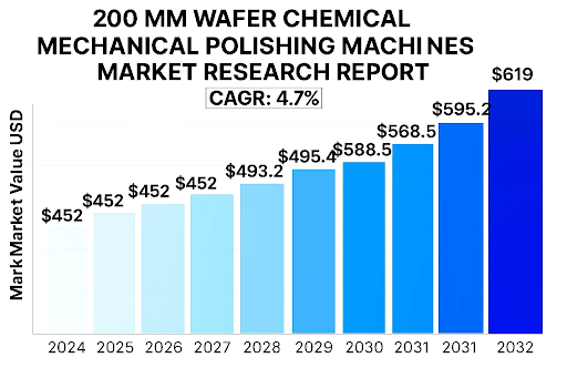
200 mm Wafer Chemical Mechanical Polishing Machines Market was valued at 452 million in 2024 and is projected to reach US$ 619 million by 2032, at a CAGR of 4.7% during the forecast period
The global 200 mm Wafer Chemical Mechanical Polishing Machines Market was valued at 452 million in 2024 and is projected to reach US$ 619 million by 2032, at a CAGR of 4.7% during the forecast period.
Chemical Mechanical Polishing (CMP) machines are critical semiconductor manufacturing tools that combine chemical and mechanical processes to planarize wafer surfaces. These systems use specialized slurries containing abrasives and reactive chemicals to remove material uniformly, enabling precise fabrication of integrated circuits. The technology is essential for achieving the nanometer-level flatness required in advanced chip production across multiple layers including copper interconnects, silicon dioxide, and tungsten plugs.
The market growth is driven by sustained demand for legacy semiconductor nodes and emerging applications in power devices, MEMS, and analog chips. While the industry has largely transitioned to 300 mm wafers for leading-edge logic, the 200 mm segment remains vital for specialized applications, with fab utilization rates exceeding 80% as of 2024. Key players like Applied Materials and Ebara Corporation continue to innovate in this space, recently introducing advanced endpoint detection and multi-zone polishing technologies to improve process control for mature nodes.
Download Free Sample Report: https://semiconductorinsight.com/download-sample-report/?product_id=103374
MARKET DRIVERS
The semiconductor industry is experiencing unprecedented capacity expansions, particularly for mature process nodes that utilize 200mm wafers. Over 20 new 200mm wafer fabs are either under construction or planned globally through 2026, creating substantial demand for chemical mechanical polishing equipment. This trend is driven by sustained demand for analog chips, power semiconductors, and MEMS devices which are predominantly manufactured on 200mm lines. Automotive electrification and industrial IoT applications are major contributors to this growth, requiring specialized semiconductors that benefit from the cost efficiency of 200mm wafer processing.
Recent Developments Reshaping the Industry
- Applied Materials Launches Mirra Durum CMP System for SiC Wafers
One of the most significant developments in recent years is Applied Materials’ release of the Mirra Durum CMP tool, targeted at 200 mm SiC wafer processing. Launched alongside the VIISta 900 hot ion implant system, this CMP platform enables:
- Support for 200 mm SiC wafers
- Improved removal rate control for hard materials
- Reduction of total cost of ownership via efficient slurry use
Why it matters: As EV powertrain inverters and fast-charging solutions increasingly rely on SiC technology, the Mirra Durum offers fab engineers a pathway to scale up without transitioning to a 300 mm line.
- Nikon’s Entrance into CMP with the NPS2301 System
In an unexpected move, Nikon—long known for lithography and metrology tools—entered the CMP market with its NPS2301 platform in 2024. Co-developed with Okamoto Machine Tool, this tool is optimized for:
- Copper/low-k dielectric planarization
- 150 mm to 200 mm wafer compatibility
- Reduced slurry consumption (up to 25%)
- 50 wafers-per-hour throughput
List of Key 200 mm Wafer CMP Machine Manufacturers Profiled
- Applied Materials, Inc. (U.S.)
- Ebara Corporation (Japan)
- Tianjin Huahaiqingke Co., Ltd. (China)
- Logitech Limited (U.K.)
- Revasum, Inc. (U.S.)
- Alpsitec S.r.l. (Italy)
Segment Analysis:
By Type
Copper CMP Machines Hold Significant Market Share Due to Extensive Use in Advanced Semiconductor Fabrication
The market is segmented based on type into:
- Copper CMP Machines
- Subtypes: Single-side and double-side polishing systems
- Silicon Oxide CMP Machines
- Front-end Tungsten CMP Machines
- Interlayer Dielectric Layer CMP Machines
- Wafer Silicon Surface CMP Machines
- Polysilicon CMP Machines
- Others
By Application
Foundry Segment Dominates the Application Landscape Due to Growing Semiconductor Manufacturing Demand
The market is segmented based on application into:
- IDM (Integrated Device Manufacturers)
- Foundry
By Technology
Advanced Node Technology Segment Grows Rapidly With Miniaturization Trends
The market is segmented based on technology into:
- Planar CMP Technology
- Advanced Node CMP Technology
- Subtypes: 45nm, 28nm, and below 28nm nodes
By Automation Level
Fully Automated Machines Gain Traction for High-Volume Production Facilities
The market is segmented based on automation level into:
- Semi-automated CMP Systems
- Fully Automated CMP Systems
Download Free Sample Report: https://semiconductorinsight.com/download-sample-report/?product_id=103374
About Us:
Semiconductorinsight has been a leading aggregator and consulting provider of semiconductor industry market research reports since 2016, offering high-quality, reliable, and timely reports and consulting services to our clients.
Services Offered
- Market Reports:
- Comprehensive and data-driven reports offering deep dives into specific segments of the semiconductor industry.
- Forecasts and trends analysis backed by robust methodologies and historical data.
- Custom Research:
- Tailored research solutions addressing unique business challenges and opportunities.
- Market entry strategies, competitive benchmarking, and M&A advisory.
CONTACT US:
City vista, 203A, Fountain Road, Ashoka Nagar, Kharadi, Pune, Maharashtra 411014
[+91 8087992013]
help@semiconductorinsight.com
The macro analyst desk brings highly sought after financial news based on market analysis, insider news and company filings.